Low-capacitance structure for operating LEDs on the AC network
In LED lighting devices (LED, Light Emitting Diode) that are operated on an alternating current supply network (AC power supply network) or are terminated, glow phenomena sometimes occur - especially with a sinusoidal voltage supply - in the off state, i.e. when the lighting devices are switched off and should therefore actually be dark.


Technical solution proposal G2016-016
Corporate entity: Diehl Aerospace GmbH
Description:
In LED lighting devices (LED, Light Emitting Diode) that are operated on an alternating current supply network (AC power supply network) or are terminated, glow phenomena sometimes occur - especially with a sinusoidal voltage supply - in the off state, i.e. when the lighting devices are switched off and should therefore actually be dark.
An LED lighting device is known, for example, from DE 10 2012 006 341 A1. The lighting device is adapted for an AC voltage supply. For this purpose, an LED lighting device for an AC voltage supply is proposed, having a plurality of LEDs which form an overall chain, the LEDs being distributed in LED subgroups, a supply voltage with alternating amplitude being present in the LED lighting device, and having a plurality of series switching devices and having a plurality of short-circuiting devices. A control device is designed to control the short-circuiting devices and the series switching devices in order to set the overall chain into at least two switching states, the at least two switching states being distinguished by the forward voltage of the overall chain.
The task of the proposed technical solution, hereinafter also referred to as the invention, is to at least reduce such glow phenomena.
The task is solved by the following light module. The light module contains a printed circuit board. The printed circuit board has a ground plane. In a switched-off state of the light module, the ground surface is connected to or has an electrical ground potential. The light module has at least one LED arrangement which is arranged on the circuit board at a distance from the ground surface.
The printed circuit board at a distance from the ground surface. Each of the LED arrangements is connected solely to an electrical supply potential in the off state. The LED arrangement thus has the supply potential at least at one point. A respective shielding surface is arranged between each of the LED arrangements and the ground plane. The shielding surface can also be designed for at least two LED arrangements together. In the off state, the shielding surface is connected to or has the electrical supply potential.
"Connected" means that the corresponding element therefore also holds the corresponding potential - if applicable at the corresponding location. The ground surface and the shielding surface are in particular flat surfaces. The surfaces run in particular parallel to each other and are arranged spaced apart. The spacing of the LED arrangement from the ground plane refers to a direction perpendicular to the ground plane or ground plane and/or to the shielding surface or shielding plane. In relation to printed circuit boards, it is also common to say that the LED arrangement is therefore arranged "above" the ground plane and also "above" the shield plane, and the shield plane is arranged "above" the ground plane.
The LED arrangement can in particular be a single LED, if necessary including corresponding connection or supply lines, or also contain several LEDs which are connected to form a corresponding arrangement, if necessary including corresponding connection or supply lines or connecting lines.
In an operating state, in particular the ground plane is still connected to the ground potential and the LED arrangement is connected to the electrical supply potential, but not only to this potential, but also - possibly via further components or circuit parts - to the ground potential or another potential, so that a drive current flows through the LED arrangement in order to operate its LEDs. In particular, in the operating state, the LED arrangement is connected between an electrical supply potential and a current sink. In the off-state, the current sink is then switched off, i.e. does not draw any current, so that the flow of operating current through the LEDs to the current sink is interrupted, but the supply potential remains applied to the LED arrangement.
The invention is based on the observation that in such light modules, with regard to the layout of the printed circuit board, LEDs as well as their connecting lines are often routed directly over a ground plane (GND). This generates a parasitic capacitance which can be sufficiently large that it can lead to a current flow through at least one of the LEDs, since the distance to the ground plane in the circuit boards is often only a few micrometres.
The invention is based on the knowledge that the cause of glow in the off-state is parasitic capacitances in the LED circuit to earth or GND, which are charged and discharged by the AC mains supply at mains frequency. This charging current leads to glow effects that can only be reduced by parallel states. However, the use of resistors is often limited by other circuit conditions and space.
The invention is based on the idea that it would be helpful if the device design reduced these parasitic capacitances as much as possible.
According to the invention, an intermediate layer (LED protective shield) is drawn in between the LED arrays (LEDs including their connecting leads) and the ground plane (GND) with the shield plane. This protective shield is connected to the potential (supply potential) of the supply voltage of the LED arrangement (especially LED chain).
The resulting capacitive short-circuit between the two supply potentials short-circuits the parasitic capacitance ("C1") between the LED array and the shield surface. In the off-state, the capacitance "C1" is ineffective, i.e. no current flows through it, since both the arrays 8a,b and the shielding surface 10, and thus both connection ends of the capacitance C1, are at the same electrical potential, i.e. the supply potential. This can therefore not cause a glow effect in the LEDs.
The parasitic capacitance ("C2") between the shielding surface and the ground surface is only charged by the mains (supply potential versus ground potential), a current does not flow through the LEDs here, which also cannot contribute to any glow effect. Only a parasitic stray capacitance ("C3") remains between the LED array and the ground potential. Due to the arrangement of the shielding surface between the LED array and the ground surface, however, the latter parasitic capacitance C3 is smaller than a parasitic capacitance ("C0") between the LED array and the ground surface without the presence of the shielding surface according to the invention with otherwise the same dimensions. The remaining parasitic capacitance C3 according to the invention between the LED arrangement and the ground plane can be designed to be significantly smaller than a corresponding comparative capacitance C0 without a shielding surface, in particular depending on the design of the layout. This means that the remaining capacitance C3 between the LED array and the ground plane, which is active in the off state and is responsible for any glow of the LED array, can be significantly reduced compared to C0.
Which at least significantly reduces or prevents the glow of the LED array in the off-state.
For example, a corresponding capacitance C3 according to the invention can be reduced to a factor of 1:16 compared to the capacitance C0 without a shielding surface between the LED arrangement and the ground potential.
According to the invention, the parasitic capacitances between the LED arrangement and the ground potential are thus reduced. Reductions of up to a factor of 1:16 compared to a conventional design are possible.
Advantages of the invention are smaller construction volumes and lower costs. The invention can even be implemented cost-neutrally, since the invention can only be implemented with the aid of suitable layout rules in a layout that is to be created anyway, without additional costs. According to the invention, the problem of glowing LEDs when the device is switched off is solved - especially when operating mains-free devices on the AC mains. However, this also applies to devices with a power supply unit.
The invention can be implemented solely by modifying or changing the layout in order to solve the glow problem in lighting devices (especially in the case of long luminaires). The glow problem can thus also be solved for light modules or light devices if there is no space for many resistors, which would be necessary to solve the glow problem alternatively.
A light module according to the invention can, for example, be used in a corresponding lighting device.
In a preferred embodiment, the printed circuit board is a multilayer printed circuit board, i.e. the printed circuit board has at least two layers in which conductors may be present. The ground plane and/or the shield plane are at least part of a respective layer of the printed circuit board. In this way, the ground plane and/or the shield plane can be implemented particularly easily in a printed circuit board or in a light module.
In a preferred embodiment, at least one of the LED arrangements has at least two connection poles. The supply potential is applied to at least two of the connection poles in the off state. In particular, the LED arrangement has exactly two connection poles and the supply potential is applied to both connection poles in the switched-off state. In particular, the entire LED arrangement is connected to the supply potential at all its terminals in the off-state. This is the most critical situation for a glow effect on the LEDs, since here the parasitic capacitances between the LED arrangement and the ground plane are supplied with the greatest possible potential difference (supply potential to ground potential) and thus the greatest possible parasitic current can flow through the LEDs.
In a preferred embodiment, at least one of the LED arrays contains at least one LED chain. The LED chain is a series connection of at least two LEDs with at least connecting lines between the LEDs and possibly before and/or after the LEDs. An LED array can have several chains in series and/or parallel connection. An LED chain is in particular an alternating series connection or direct series connection of LEDs and interconnected line sections without the interconnection of other components. Alternatively, the LED arrangement also contains further electrical components which are connected to at least one of the LEDs or connecting lines. Such components are, for example, further feed lines, open-circuit diodes, resistors, etc. Such LED chains are particularly susceptible to glow phenomena.
In particular, the "simple" LED chains, which consist solely of LEDs and connecting lines, do not contain any protective devices against glow phenomena, but are simple and inexpensive and can nevertheless be effectively protected against glow phenomena thanks to the invention.
In a preferred variant of this embodiment, at least one of the LED chains has a switchable parallel bypass between its ends, which short-circuits the LED chain between its ends in the off state. In the simplest case, the bypass is an interruptible connecting line between the ends of the LED chain. The "ends" are the section from the last LED of the chain to the respective connection point of the chain. This results in the two ends of the LED chain having the same electrical potential, in particular the supply potential, in the off state. In this case, glow phenomena are particularly probable due to the applied supply potential and can thus still be prevented by the invention.
In particular, each of the LED chains has such a parallel bypass. In operation, the parallel bypass is open or short-circuited, usually in alternating operation. For LED arrays with such LED chains, a lighting device results in particular from a corresponding circuitry of one or more light modules, in that respective series connection of light chains with parallel bypass are connected at one end to the supply potential and at the other end to earth via controlled current sources. Thanks to the invention, glow phenomena in the off-state can also be effectively reduced in such lighting devices.
In a preferred variant of this embodiment, at least one, in particular each, of the LED chains contains LEDs of the same light colour, i.e. the colour of the light emitted during regular operation. In particular, at least two LED chains of different light colours are present in a light module or light device. In this way, multi-colour light modules or multi-colour light devices can be created. Light colours are in particular W, R, G, B (white, red, green, blue). In particular, in one or more of the LED arrangements, all LEDs are white and/or in one or more of the LED arrangements, light chains - in particular, the same number of chains and/or LEDs - of the colours R, G and B, possibly also of the colour W, are contained. This results in W, RGB or RGBW LED arrangements.
In a preferred embodiment, a projection space is assigned to each of the LED arrangements. The projection space is a perpendicular projection of the (geometry of the) LED array onto the ground plane. The screen surface completely fills the projection space in cross-section. This means that at least almost the entire area resulting from the intersection of the plane of the screen surface with the projection space is actually filled by the screen surface. "Almost" means that only, for example, through-contacts, component connections, lines that do not interfere with the glow effect or similar are included in the cross-sectional area. In particular, the screen surface fills the corresponding cross-section or projection space at least completely or over the entire surface, or at least partially even projects laterally beyond it (in relation to the perpendicular to the ground surface).
In a special embodiment, the light module has a corridor in which at least one of the LED arrangements runs. In particular, all LED arrangements run within this corridor. The corridor can be two-dimensional or spatially extended. A projection space is also assigned to the corridor, which is a perpendicular projection of the corridor onto the ground plane. The screen surface then - in the sense explained above - also fills this projection space in cross-section.
The light module extends in particular along a longitudinal direction, i.e. it is an elongated light module. In particular, at least one, preferably all, LED arrangements then also run along this longitudinal direction and/or within the corridor. "Along the longitudinal direction" refers to its basic direction of extension, whereby the arrangements can also run crossed, twisted, etc. in a 3D structure. The projection space is therefore related to the entire corridor, including any spaces between LED arrangements. The screen surface is thus located between the corridor and the ground plane and refers to the entire corridor, in particular the LED arrangements or LED chains guided therein.
In a preferred variant of this embodiment, the corridor is bordered laterally by each LED arrangement. In other words, the corridor extends in such a way that the outermost LED arrays are just contained within it.
The corridor thus has the smallest possible shape for given LED arrangements.
In a preferred variant of this embodiment, the screen surface projects laterally beyond the projection space or spaces by at least a minimum amount. "Laterally" here means as above: seen in a plane parallel to the ground plane, away from the respective LED arrangement or corridor or their projection. This results in a respective lateral minimum projection over the respective projection spaces. In other words, a vertical projection of the LED arrangement or the corridor onto the ground surface defines a spatial area and the screen surface projects laterally with the minimum projection beyond the side surfaces of the spatial area. Such a projection is in particular 0.5-1.5mm, in particular 0.8-1.0mm, in particular 0.9mm.
In a preferred variant of this embodiment, the light module contains at least one further electrical component. Each of the components is laterally spaced from the screen surface by at least a minimum dimension with respect to its projection space (which is again analogously as set out above). In particular, this minimum dimension is the same minimum dimension as above. The lateral distance of the electrical components from any component of the LED arrangement is therefore at least the sum of both minimum dimensions (in case of equality, double the minimum dimension). This does not apply to components that cannot contribute to the glow effect of the LEDs, e.g. are located beyond the shielding surface and/or the ground plane from the point of view of the LED arrays.
In a preferred embodiment, the shielding surface has a minimum perpendicular distance to the ground plane. "Perpendicular" refers mutatis mutandis as above to the ground plane or screen plane. The minimum distance determines the parasitic capacitance between the shielding surface and the ground plane and thus limits this capacitance to a maximum.
In a preferred embodiment of the invention, the light module has a minimum dimension defined above. The minimum distance then corresponds to at least half the minimum dimension. In particular, the minimum distance then corresponds to 0.25-0.75mm, in particular 0.4-0.5mm, in particular 0.45mm.
In a preferred embodiment, the light module is a light module for interior lighting of an aircraft. The invention is particularly effective for such light modules in aircraft, since it can be achieved solely by changing the layout of the printed circuit board.
And does not require any other components, so that, as mentioned above, above all a low weight results for the light module, which is particularly advantageous for use in aircraft.
The task of the invention is also solved by a lighting device. The lighting device and at least some of its embodiments, as well as the respective advantages, have already been explained analogously in connection with the lighting module according to the invention.
The light device has at least one light module according to the invention.
In a preferred embodiment, each of the light modules is connected with respect to its LED arrangement on the one hand to the electrical supply potential and on the other hand via a current sink to the earth potential. In particular, at least two light modules and thus also their LED arrangements are connected in parallel. The lighting device is in particular a transformerless device in which direct operation on the mains is possible. Alternatively, the lighting device is a lighting device with a power supply unit. In particular, the light module contains the above-mentioned switchable parallel bypasses, which are then controlled by a controller of the light device in order to operate the LED arrays as desired (in terms of colour and/or brightness).
For such particularly simple lighting devices, the invention can be implemented in a particularly cost-effective and weight-saving manner, which leads to the above-mentioned advantages.
The invention is based on the following findings, observations or considerations and also has the following embodiments. The embodiments are also referred to in part as "the invention" for the sake of simplicity. The embodiments may also contain or correspond to parts or combinations of the above-mentioned embodiments and/or may also include embodiments not previously mentioned.
The invention is concerned with the problem that in LED lighting devices on the AC mains in the off-state - caused by parasitic capacitances and the AC voltage applied - equalising currents occur between the LEDs and the housing, which lead to glow phenomena. These phenomena can also occur during operation with a power supply running on the supply voltage.
Within the scope of the invention, a method or device is presented with the aid of which it is possible to keep the parasitic capacitances as small as possible when LEDs are operated on the AC supply voltage (either in direct operation or via a power supply unit), so that glow in the off-state can be minimised. With the design concept according to the invention, the parasitic capacitances and thus also the glow currents and the glow phenomena are reduced.
In accordance with the invention, a low-capacitance structure for operating LEDs on the AC mains is obtained. According to the invention, the development of extremely low-cost and/or smaller lighting devices for aircraft is possible.
Further features, effects and advantages of the invention will be apparent from the following description of a preferred embodiment of the invention and the accompanying figures. A schematic sketch shows the principle of the invention:
Figur 1 a light module in cross-section,
Figur 2 a structure of a light unit with light module with circuit diagram,
Figur 3 an alternative light module in cross-section.
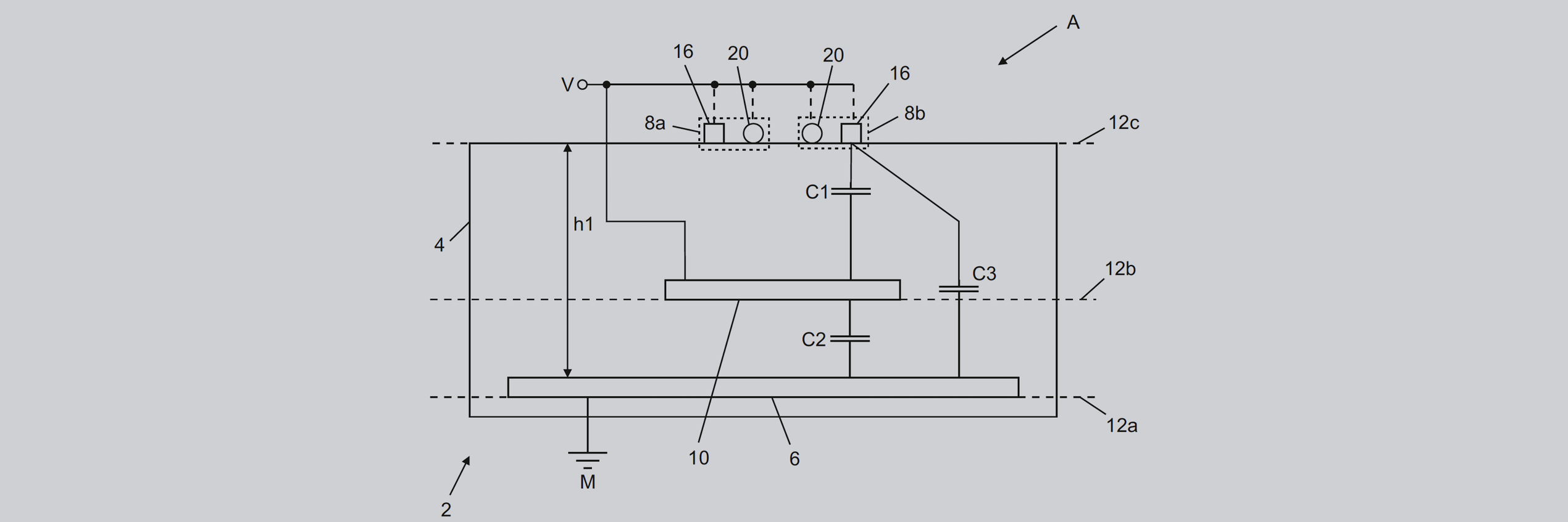
Figure 1 shows a cross-section of a light module 2 extending longitudinally perpendicular to the drawing plane, which contains a printed circuit board 4. The circuit board 4 contains a ground plane 6, which is flat in this case. The light module 2 is shown in a switched-off state A. The ground plane 6 is connected to or has an electrical ground potential M in the switch-off state A of the light module 2.
Two LED arrangements 8a,b are arranged on the printed circuit board 4 at a distance h1 from the ground plane 6. In the off-state A, each of the LED arrangements 8a,b is connected solely to an electrical supply potential V; this is shown in Figure 1 only symbolically by a dashed line. A shielding surface 10 is arranged between each of the LED arrays 8a,b and the ground plane 6. This is also flat and runs parallel to the ground plane 6. In the switch-off state A, it is connected to the electrical supply potential V or has this. In the example, the shielding surface 10 is even continuous for both arrangements 8a,b.
The printed circuit board 4 is a multilayer printed circuit board with a total of three layers 12a-c, whereby the ground plane 6 lies on the layer 12a, the shielding surface 10 on the layer 12b and the LED arrangements 8a,b on the layer 12c or form at least a part of the respective layer 12a-c.
In the arrangement, the parasitic capacitances:
- C1 between the respective arrangement 8a,b and the shielding surface 10,
- C2 between the shielding surface 10 and the ground plane 6,
- C3 between the respective arrangement 8a,b and the ground plane 6.
In the off-state, the capacitance C1 is ineffective, i.e. no current flows through it, since both the arrangements 8a,b and the shielding surface 10, and thus both terminal ends of the capacitance C1, are at the same electrical potential, namely the supply potential.
Figure 2 shows only symbolically a lighting device 36 in the interior 32 of an aircraft 34. The lighting device contains the lighting module 2 from Figure 1. The lighting module 2 is therefore a lighting module for interior lighting of the interior 32 of the aircraft 34. The LED arrangements 8a,b are shown symbolically on the upper side or layer 12c of the printed circuit board 4. Each of the LED arrays 8a,b contains six LED strings 14a-f and 14g-l respectively, with some of the LED strings 14a-l being indicated by a dashed frame as an example. Each of the LED chains 14a-l is a series connection of ten LEDs 16 each, which are connected by connecting lines 18. Each of the serial LED arrays 8a,b has two connection poles 19a,b at its two ends.
Each of the LED chains 14a-l contains a switchable parallel bypass 20 which can either conductively connect the respective ends of the LED chains 14a-l or not. For this purpose, a corresponding switch 22 is closed or opened. In the off-state A, each of the parallel bypasses 20 short-circuits the respective ends of the respective LED chain 14a-l. Figure 1 symbolically shows the LED arrangements 8a,b in cross-section, namely one LED 16 and one parallel bypass 20 each.
Each of the LED chains 14a-l contains ten LEDs 16 of the same light colour. Thus, all LEDs 16 in the LED array 8a are white LEDs, i.e. emit white light in regular operation, the switches 20 are controlled in this case according to a method not explained in more detail in order to set a certain voltage at the LED array 8a. The LEDs of the LED strings 14g and 14j are LEDs of red light colour, those of the LED strings 14h and 14k of green light colour and those of the LED strings 14i and 14l of blue light colour. In operation, the LED array 8a therefore emits white light, and the LED array 8b emits any RGB mixed colour, depending on the control of the respective switches 22 in the LED array 8b.
In the lighting device 36, the LED arrangements 8a, b are connected on the one hand, i.e. with their connection poles 19a to the electrical supply potential V. On the other hand, the LED arrangements 8b are connected to the electrical supply potential V with their connection poles 19a. On the other hand, i.e. with their connection poles 19b, the respective LED arrangement 8a,b is connected to the earth potential M via a respective current sink 38a,b. The current sink 38a,b is in this case a respective individually controlled current source which is active in the operating state of the light unit 36 or of the light module 2 and controls an operating current through the respective LED arrangement 8a,b. This is necessary for regular operation of the light unit 36 or of the light module 2. This is responsible for the regular operation of the LEDs so that they emit light. In the off-state A, the current sinks 38a,b are switched off, i.e. they have a current flow of zero.
In the off-state A, all bypasses are also closed, which is why the supply potential V is present at both connection poles 19a,b and at each end of each LED chain 14a-l respectively.
Figure 3 shows an alternative light module 2 which, as in Figure 1, extends longitudinally perpendicular to the plane of the line and in which the printed circuit board 4 has a total of five layers 12a-e. Here the ground plane 6 is arranged on layer 12b and the shielding surface 10 on layer 12c. A total of four LED arrays 8a-d are each arranged with respect to their LEDs 16 and connecting leads 18 on layer 12e and their parallel bypasses 20 on layer 12d.
Each of the LED arrays 8a-d is associated with a respective projection space 24a-d, which is a perpendicular projection of the respective LED array 8a-d onto the ground plane 6. The screen surface 10 completely fills the respective projection space 24a-d in each case in cross-section, i.e. on the respective intersection of the layer 12c with the respective projection space 24a-d.
The light module 2 also has a corridor 24, indicated by dashed lines, which also extends longitudinally perpendicular to the drawing plane. Laterally, i.e. on its sides 28, the corridor 26 is bounded by the respective LED arrangement 8a,d. Also associated with the corridor 26 is a projection space 24, which is a perpendicular projection of the corridor 26 onto the ground plane 6. The screen surface 10 also fills this projection space 24e in cross-section (as described above). Thus, in position 12c, the spaces between the respective projection spaces 24a-d are also filled with the screening surface 10. The screen surface 10 also projects laterally beyond the projection space 24e in each case by at least a minimum dimension Mmin, in the example 0.9mm.
The light module 2 contains further electrical components 30, in the example all signal lines, which do not belong to the LED arrangements 8a-d. The projection space 24f of each of the components 30, which is only indicated, is spaced laterally from the screen surface 10 by the minimum dimension Mmin. This does not apply to components that lie beyond, i.e. below, the ground plane 6 with respect to the LED arrays 8a-d.
The screen surface 10 also has a vertical minimum distance Amin, here 0.45mm, to the ground surface 6, which thus corresponds to half the minimum dimension Mmin.
List of reference signs
2 Light module
4 Printed circuit board
6 Ground plane
8a-d LED arrangement
10 Shielding surface
12a-c Position
14a-l LED chain
16 LED
18 Connection cable
19a,b Connection Pole
20 Parallel bypass
22 Switch
24a-f Projection room
26 Corridor
28 Side
30 Component
32 Interior
34 Aircraft
36 Light unit
38a,b Current sink
A Switch-off state
h1 Distance
Mmin Minimum distance
Amin Minimum distance
V Supply potential
M Earth potential
C1-3 Capacity